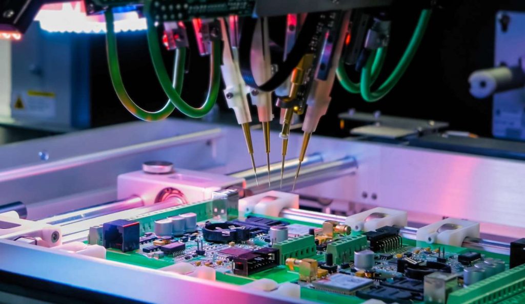
How to solder a double layer circuit board?

With the development of high-tech, people need high-performance, small-size, multi-functional electronic products, and promote the development of printed circuit board manufacturing in the direction of light, thin, short and small. Double-sided panels have electronics on both sides, making them smaller, lighter, and more portable than single-sided panels. So, do you know what the manual soldering method for double-sided pcb boards is? Next, FS PCBA will give you a comprehensive explanation of the manual soldering method of double-sided circuit boards.

Manual soldering method of double-sided PCB
1. The device to be formed should be processed according to the requirements of the process drawing; that is, it should be shaped first and then inserted.
2. After shaping, the model side of the diode should be facing up and both pins should be the same length.
3. When FS PCBA will insert a device with polarity requirements, it should be noted that the polarity cannot be reversed. After insertion, there should be no significant vertical or horizontal tilt of the roller manifold assembly.
If you feel that it is troublesome to solder double-layer circuit boards, you can try one-stop pcb assembly and manufacturing services. Beyond the most basic services, FS can also provide you with pcb component procurement services.
4. Soldering iron power for double-sided pcb board soldering is between 25-40W. The temperature of the soldering iron tip should be controlled around 242°C. If the temperature is too high, the head can easily "die". If the temperature is too low, the solder cannot melt. The time is controlled at 3-4 seconds. Strict temperature control is the key to success, and FS PCBA can be said to be an expert in this area.
5. During formal welding, generally follow the welding principle of equipment from short to high and from inside to outside. Welding time should be mastered. If the time is too long, the device will be scalded, and the copper-clad wire on the CCL will also be scalded.
6. Because it is double-sided soldering, it is necessary to make a process frame to place the pcb to avoid tilting of the devices below.
7. FSPCB will comprehensively check the quantity and seat type after the circuit board is soldered, and check the places with leakage and leakage. After confirming that it is correct, trim the redundant device pins on the circuit board, etc., and then flow to the next process.
8. In the specific operation, the relevant process standards should also be strictly followed to ensure the welding quality of the products.
The above are all the steps of FS PCBA in the production of double-layer circuit boards, I hope it can help you.
FS Technology is the most famous pcba company in China. We not only provide pcb manufacturing and pcb assembly services, but also have compiled pcb knowledge for the majority of pcb industry practitioners. If you are also interested in this industry, then come to FS Technology's blog to learn.